What Can It Run?
Demo programs running on the CPU: iterative Fibonacci (left) and prime number sieve (right).
Both use the CPU's stack, I/O, and arithmetic instructions.
Project Overview
- Goal: design and implement a fully functional single-cycle 16-bit RISC CPU in Logisim
- Implemented the Duke 250/16 ISA (inspired by MIPS ISA): 16 instructions across R, I, and J formats
- Wired a full datapath with combinational control logic
- Built from primitive components (logic gates, multiplexers, D flip-flops)
- Harvard architecture: separate 16-bit ROM (instruction memory) and RAM (data memory), word-addressed
- Automated test suite: 9 / 9 test programs passed, including recursion, I/O, shifts, memory, and branch/jump instructions
CPU Architecture
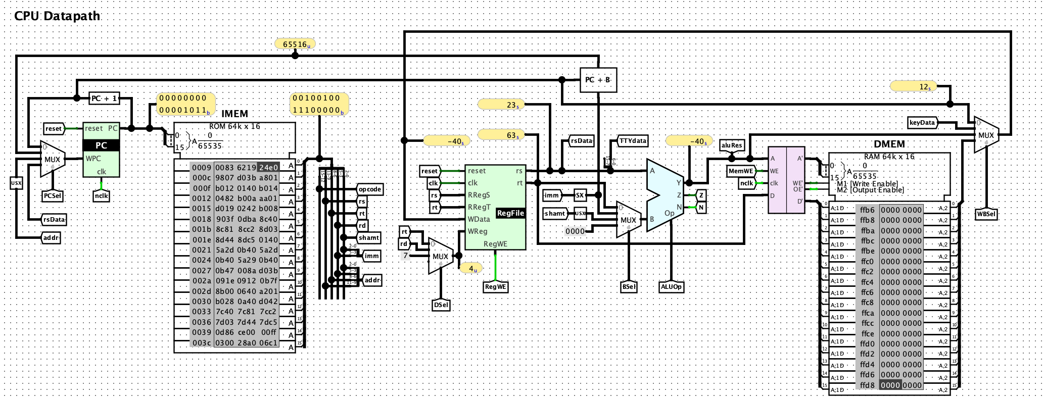
The CPU follows a classic single-cycle RISC datapath: each instruction completes within one clock cycle, with all datapath decisions made combinationally from the opcode. The design uses a Harvard architecture (instruction and data memory are separate) which maps naturally to Logisim's ROM (instruction fetch) and RAM (load/store) components.
Subcircuits
The CPU is decomposed into reusable subcircuits. Each was designed and tested independently before being wired into the main datapath.
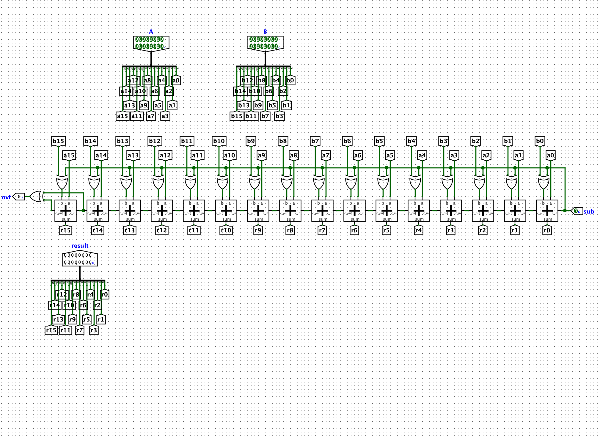
Arithmetic Logic Unit
- 7 operations: ADD, SUB, NOT, AND, SLL, SRL
- 3-bit
ALUOpselect input drives a MUX over operation outputs - Zero flag output used by
beqto detect equality - Sign-bit output used by
bgezto detect ≥ 0
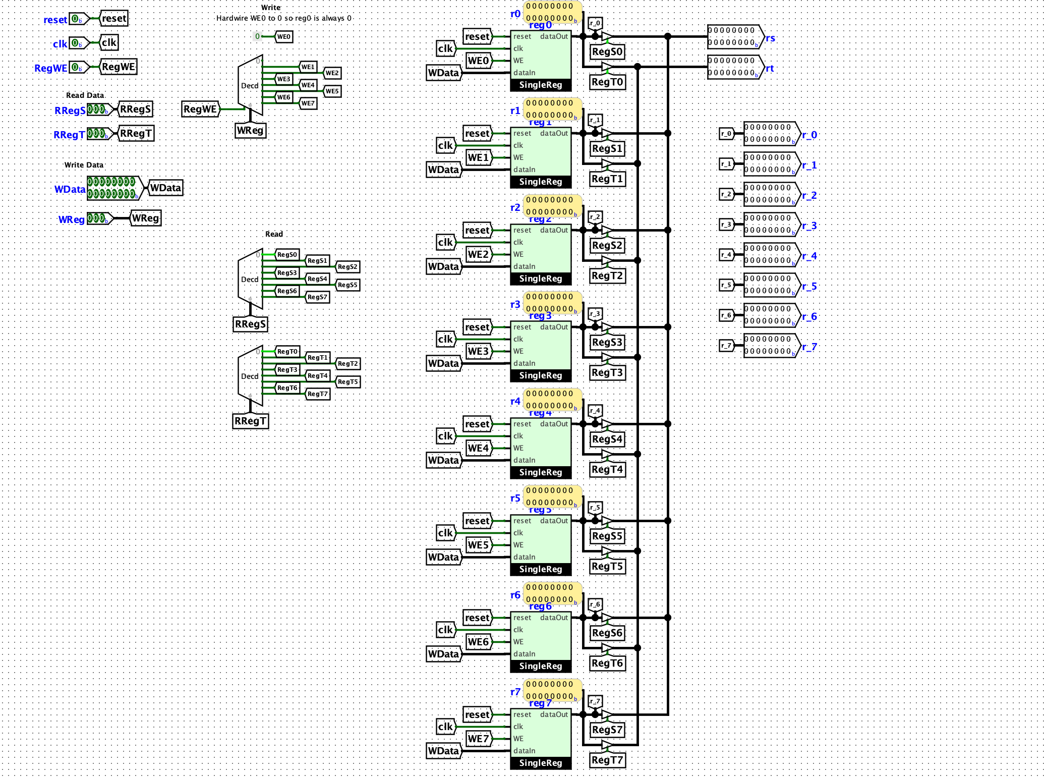
Register File
- 8 × 16-bit registers ($r0–$r7); $r0 hardwired to zero
- Read ports use tri-state buffers + decoder
- Write port clocked on rising edge; $r0 write-enable permanently disabled
- Asynchronous reset clears all registers via DFF clear pins
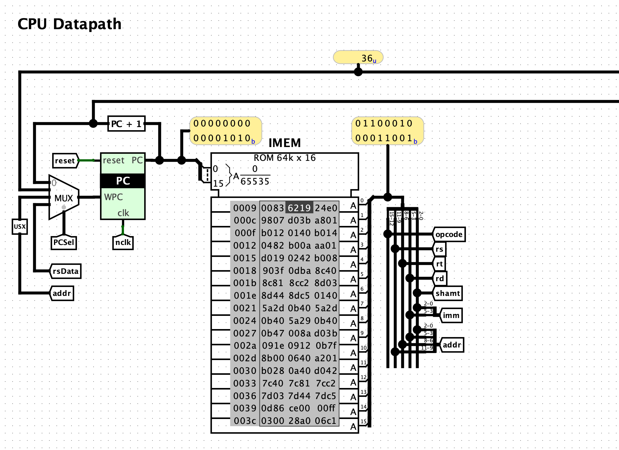
PC Logic
- PC register clocked on falling edge (inverted clock) for timing correctness
- 2-bit
PCSelchooses next PC: sequential (PC+1), branch (PC+1+B), jump (J-addr), or register ($rs) - Branch condition (Zero/Sign flag from ALU) gates whether branch target is selected
- Asynchronous reset forces PC to 0x0000
Control Signals
A central control unit decodes the 4-bit opcode and drives 9 control signals that route data through the datapath each cycle.
PCSel selects the next PC source; DSel picks the destination register; RegWE enables register writes;
BSel selects ALU input B; ALUOp sets the ALU operation; MemWE enables memory writes;
WBSel selects the write-back data; keyRE enables keyboard read; TTYWE enables TTY write.
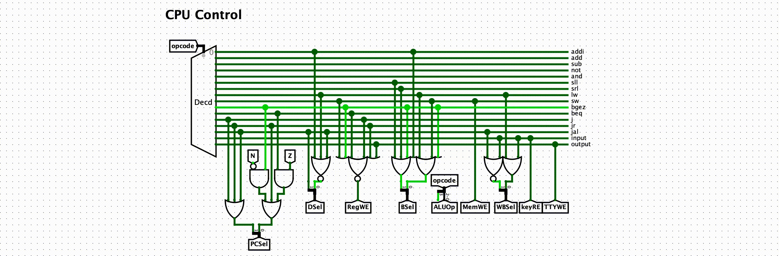
| Instruction | PCSel | DSel | RegWE | BSel | ALUOp | MemWE | WBSel | keyRE | TTYWE |
|---|---|---|---|---|---|---|---|---|---|
addi | 00 | rt | 1 | imm | add | 0 | alu | 0 | 0 |
add | 00 | rd | 1 | rt | add | 0 | alu | 0 | 0 |
sub | 00 | rd | 1 | rt | sub | 0 | alu | 0 | 0 |
not | 00 | rd | 1 | rt | not | 0 | alu | 0 | 0 |
and | 00 | rd | 1 | rt | and | 0 | alu | 0 | 0 |
sll | 00 | rd | 1 | shamt | sll | 0 | alu | 0 | 0 |
srl | 00 | rd | 1 | shamt | srl | 0 | alu | 0 | 0 |
lw | 00 | rt | 1 | imm | add | 0 | mem | 0 | 0 |
sw | 00 | — | 0 | imm | add | 1 | — | 0 | 0 |
bgez | 01 | — | 0 | 0 | add | 0 | — | 0 | 0 |
beq | 01 | — | 0 | rt | sub | 0 | — | 0 | 0 |
j | 10 | — | 0 | — | — | 0 | — | 0 | 0 |
jr | 11 | — | 0 | — | — | 0 | — | 0 | 0 |
jal | 10 | r7 | 1 | — | — | 0 | PC+1 | 0 | 0 |
input | 00 | rd | 1 | — | — | 0 | key | 1 | 0 |
output | 00 | — | 0 | — | — | 0 | — | 0 | 1 |